
LIONTEC Dotting Inkjet System delivers ultra‑precision dot marking for semiconductor and optical component manufacturing.LIONTEC high‑precision wafer inkjet printer and dotting system integrates machine vision and piezoelectric inkjet technology to realize sub‑micron automatic black‑out marking for wafer defects. It breaks through the efficiency bottleneck of traditional manual operation, meets mass‑production requirements of optical components such as ToF modules and metalenses, and provides highly reliable marking solutions for 3D sensing and biometric identification fields.
High‑Precision Dotting Inkjet System for Semiconductor Wafers
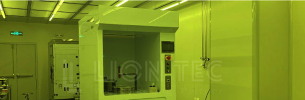
A [Machine Vision Positioning] | Sub‑micron Recognition Accuracy | → B (Defect Coordinate Extraction) → C [Piezoelectric Inkjet System] | 3pl‑level Droplet Control | → D (Micron‑level Precision Dotting) → E [SECS/GEM Protocol Integration] → F (Seamless Connection with Intelligent Manufacturing System)
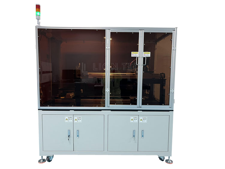
Three Core Technical Modules of Ultra‑High Precision Dotting System
-
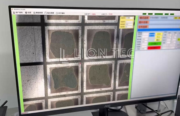
Industrial Vision Recognition System
Millisecond‑level defective product positioning (frame rate >500fps)
Sub‑micron coordinate positioning error (≤2 μm)
LIONTEC integrates a wide range of eco‑friendly inks with advanced and secure variable‑data marking software to deliver a highly competitive total solution.
-
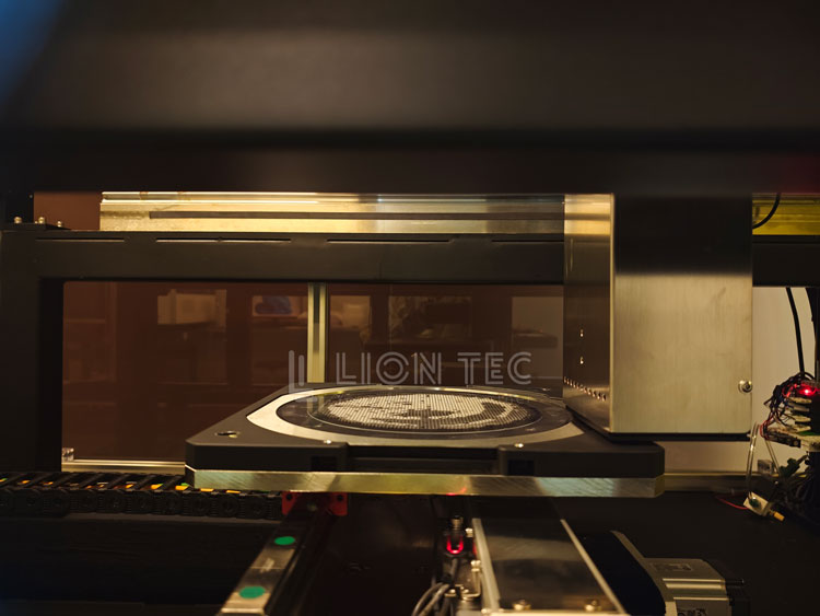
Piezoelectric Inkjet Execution System
Nano‑level droplet volume control (3‑5 pl)
High‑adhesion semiconductor‑specific ink (resistant to cutting fluid & high temperature)
-
Intelligent Control Platform
SMEMA/E84 protocol compatible
Customizable formula management (>200 process parameter groups)
Deployed in 12‑inch wafer mass‑production lines, it delivers core marking technology for 3D imaging, biometrics and other advanced sectors, advancing the domestic development of semiconductor inkjet equipment.
Application Areas
- Mass Production of Optical Components:Defect Marking for ToF Modules & Metalenses
- 3D Sensing Chips:Dotting & Positioning for Structured Light Receivers
- Biometric Identification Devices:Wafer‑level Grading for Fingerprint Sensors
Online Message
We would be glad to help you find the best coding and marking solution to fit your requirements.