
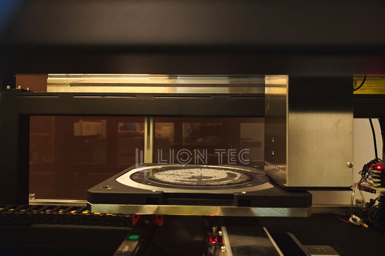
Semiconductor Wafer Glass Inkjet Dotting for Defect Marking, Replace Traditional Probe Marking
LIONTEC high-precision wafer dotting inkjet system addresses the production challenge where manual black marking of defective products used in R&D and testing is no longer suitable for mass production, as most equipment fails to achieve ultra-fine marking. It enables automatic and efficient identification of defective wafers, realizing seamless integration of high-precision, highly reliable black marking.…